To say that semiconductor expertise is a part of the material of contemporary society will not be an overstatement—it underpins every thing from our automobiles to our telephones to our house home equipment. In 2021, the semiconductor trade shipped a report 1.15 trillion chips, and gross sales topped half a trillion {dollars} worldwide, whereas hundreds of latest chip designs entered the market.
A brand new semiconductor chip structure, termed “multi-die system” or “chiplet-based design,” shall be instrumental in assembly this decade’s burgeoning demand for processing energy. As a result of this new strategy will pose technical challenges all through the semiconductor ecosystem—remaking how merchandise are imagined, designed, and fabricated—alternatives for innovators throughout the worth chain will emerge from this shift. Enterprise leaders throughout industries who establish use instances for these superior chips will profit from their capability to energy distinctive and customised buyer experiences.
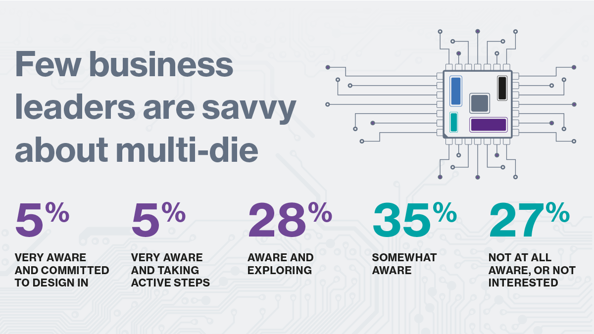
Few enterprise leaders, nevertheless, are holding tempo with the newest developments on this area. Multi-die expertise continues to be an enigma to many executives. A current ballot by MIT Expertise Assessment Insights requested enterprise leaders about their consciousness of this design technique—and located that 62% of respondents are both uninterested, unaware, or solely considerably conscious of this expertise’s capabilities.
A number of chip-reliant industries clearly have to maintain a detailed eye on developments in semiconductor tech: automotive corporations, synthetic intelligence companies, hyperscale information processing organizations, and sensible system producers, to call a couple of. However as a result of superior semiconductors are foundational to modern-day enterprise operations, even executives whose features don’t straight contact expertise ought to care about chip design traits—together with these that may outline the sector’s subsequent chapter.
Why semiconductors matter
Whereas the worldwide semiconductor scarcity that started in 2020 had its proximate causes in pure disasters and geopolitics, its results drew widespread consideration to the truth that nearly each trade depends on chips. And pandemic-related ripple results apart, the silicon establishment has been in flux for a while. New applied sciences like synthetic intelligence and machine studying (AI/ML), which require better computing effectivity and efficiency, have strained conventional methods lately.
With the rise of the Web of Issues (IoT), prospects have additionally come to count on intelligence in every thing from fridges to lightbulbs. Innovators are responding accordingly. Our ballot discovered that just about one-third (31%) of enterprise executives plan to enhance upon their corporations’ current sensible merchandise, and nearly one other third (29%) intend so as to add AI/ML capabilities to their merchandise quickly. Solely 9% of respondents mentioned they weren’t producing IoT or linked units.
This sort of expertise, nevertheless, necessitates strong edge computing and on-device processing, which requires better and extra environment friendly {hardware} efficiency. Complicating issues, the cloud information facilities powering this compute shift are additionally voracious vitality shoppers. That is one other space the place conventional silicon is stagnating: sustainability. The price of producing superfluous silicon isn’t just unhealthy for enterprise—it has an environmental influence. And whereas there’s an ongoing push towards net-zero carbon emissions inside the semiconductor provide chain, the trade isn’t but on observe to satisfy the emissions requirements set forth within the UN 2016 Paris Settlement.
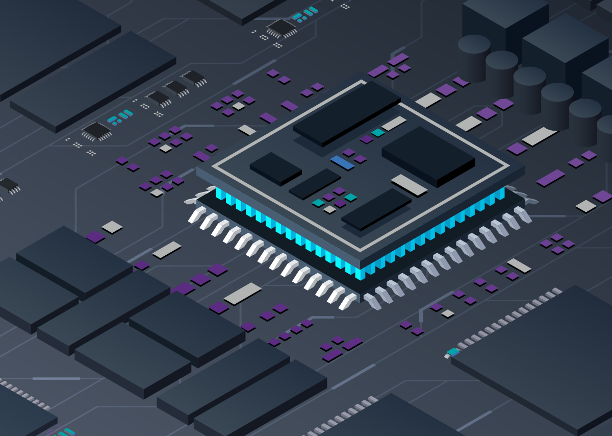
An trade shift towards multi-die design could possibly be a part of the answer to those challenges. As an alternative of a single monolithic chip (“system on chip”), multi-die designs encompass a set of chips (chiplets or dies) linked in a complicated package deal (“methods of chips”), which may embody stacking blocks in a 3D configuration for better density. Multi-die system designs are able to supporting the rollout of AI/ML at scale, and so they can enhance silicon yields, decreasing waste throughout chip manufacturing.
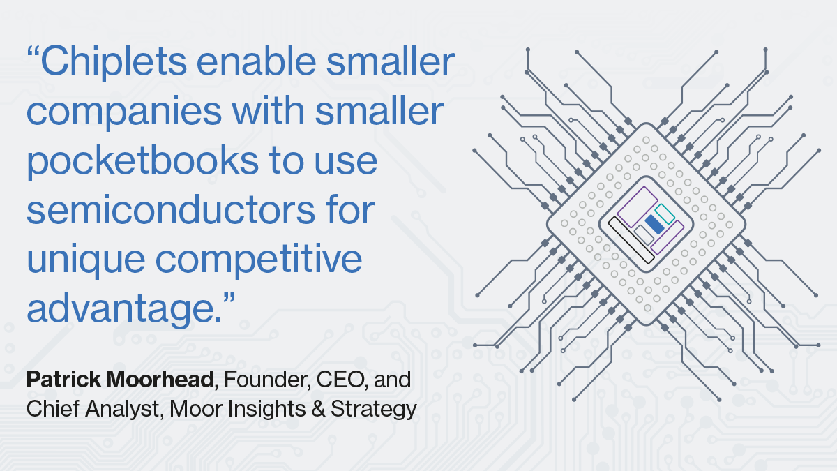
In the case of the enterprise use instances for multi-die methods, Patrick Moorhead, founder, CEO, and chief analyst at international expertise consulting agency Moor Insights & Technique, notes that these customized designs might quickly be a key differentiator for corporations seeking to stand out amongst rivals. “As extra individuals are taking a look at extra customized silicon as a option to differentiate what they create to the desk, that’s what businesspeople must be taking a look at,” he says. “Chiplets allow smaller corporations with smaller pocketbooks to make use of semiconductors for distinctive aggressive benefit.”
Gerry Talbot, a company fellow at semiconductor firm AMD, boils the enterprise worth of chiplets right down to the big selection of use instances for the expertise. “I don’t assume [business leaders] shall be so excited in regards to the expertise itself,” he says, “as a lot as the applying and the enablement of a singular consumer expertise that may assist promote their product.”
Obtain the report.
This content material was produced by Insights, the customized content material arm of MIT Expertise Assessment. It was not written by MIT Expertise Assessment’s editorial workers.


